Intel said on July 24 that it is collaborating with Lens Technology on advanced semiconductor packaging for the AI era. At first glance that sounds like a niche manufacturing announcement, but it points at one of the more important structural changes in modern chip design.
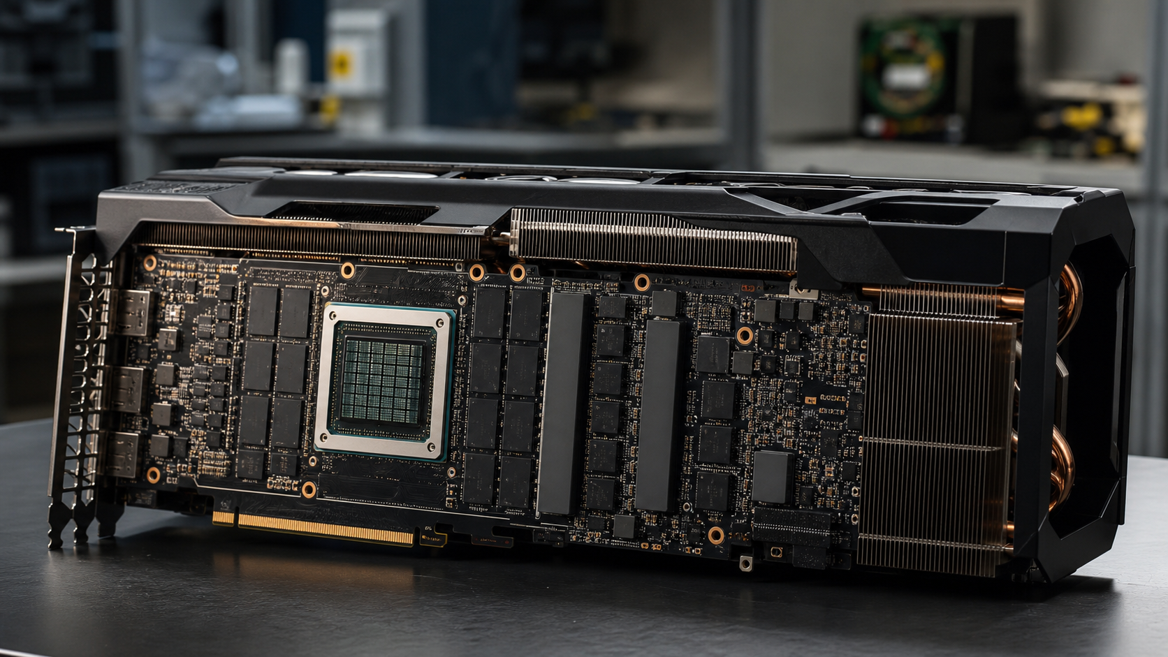
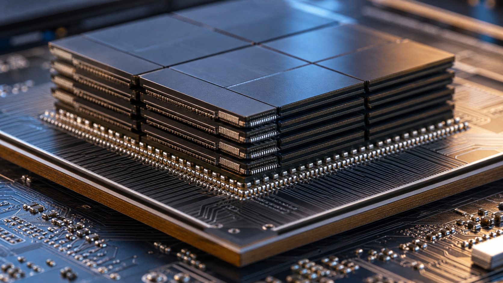
As process shrinks become more difficult and expensive, chipmakers are getting more value from how dies are connected, stacked, cooled, and integrated. Packaging is no longer just the shell around the silicon. It is increasingly the bridge between performance ambitions and the physical limits of power, thermals, signal integrity, and memory access.
That is especially true in AI infrastructure, where designers are trying to move larger models and larger datasets through increasingly complex systems. Better packaging can improve density, bandwidth, and efficiency while making multi-die designs more practical. In other words, it is one of the hidden levers that can decide whether a chip architecture works in production at scale.
Intel has strong reasons to emphasize this area. Advanced packaging is one of the company’s clearest opportunities to differentiate across foundry and systems work, even when conventional node competition remains intense. If the market keeps moving toward chiplets, stacked memory, and tightly integrated accelerators, packaging becomes a strategic battleground, not just a manufacturing footnote.
For normal readers, the headline takeaway is that future “chip wars” will not be decided purely by transistor counts. The companies that master how components are assembled into practical, high-bandwidth systems will have a real advantage, especially in AI and data-center hardware.
Why it matters: advanced packaging is moving from back-end engineering detail to front-page hardware strategy.
Source: Intel Newsroom, July 24, 2026 - Intel and Lens Technology Collaborate to Enable Advanced Semiconductor Packaging for the AI Era